Home > Product > DCS control system > LAM 853-227247-001 Robot Kit


LAM 853-227247-001 Robot Kit
- Goods status: new/used
- Delivery date: stock
- The quality assurance period: 365 days
- Phone/WhatsApp/WeChat:+86 15270269218
- Email:stodcdcs@gmail.com
- Tags:
- Get the latest price:Click to consult
LAM 853-227247-001 Robot Kit
Product Details Introduction
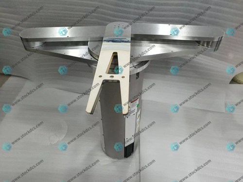
The LAM 853-227247-001 robot kit is mainly used in the semiconductor manufacturing field, especially in wafer processing, to achieve precise and efficient automated wafer transfer. It is an important component in Lam Research equipment, suitable for both Front End and Back End processes, ensuring high precision and reliability in the production process.
Product application areas
Semiconductor Manufacturing (Wafer Processing)
Lithography: In the photolithography process, the wafer needs to be accurately fed into the lithography machine and removed to ensure alignment and lossless transmission.
Etching: Used for plasma etching (such as Lam Research 9400, TCP 9600, Versys, etc.) to accurately transport wafers and avoid particle contamination.
Deposition: Suitable for chemical vapor deposition (CVD), atomic layer deposition (ALD), and physical vapor deposition (PVD) equipment to ensure uniform processing.
Ion implantation: Sending wafers from a transport system into an ion implantation machine to ensure precise alignment and improve process control capabilities.
Cleaning: Cooperate with cleaning equipment (such as SPTS Omega series) to safely handle ultra-thin wafers and prevent damage.
Flat Panel Display (FPD)
Suitable for manufacturing OLED, LCD, and MicroLED panels, ensuring precise transmission of large-sized glass substrates and preventing scratches and dust pollution.
Advanced Packaging
Used for automated handling of wafer level packaging (WLP), flip chip, and other production lines in 2.5D and 3D IC packaging processes.
Other high-precision automation
Optical communication MEMS、 Power semiconductor manufacturing: supports high-precision chip transmission and is suitable for special processes of materials such as SiC and GaN.
Laboratory automation: used for scientific research equipment, providing precise sample handling solutions.
Main advantages
High precision transmission (nanometer level alignment accuracy, avoiding wafer damage)
Clean and dust-free design (compliant with Class 1 standard for semiconductor cleanrooms)
High throughput (improving wafer handling speed and increasing production capacity)
Compatible with Lam Research equipment (suitable for core processes such as Lam etching and deposition)
Product imag

Related website links
Kollmorgen 6SM37M-6000 servo motor
Radisys ATCA-PP81 controller module
AMAT 0190-24282 encoder module
Other website links
BENTLY 1900/55 190055-0Z-01-01-01地震监测模块
| PFEL113 | 6SC6000-0NA02 | MC-PDOY22 80363975-150 |
| PFEL111 | 6SC6140-0FE01 | MC-PD1X02 |
| PFEA113 | 6SC6500-0UC01 | MC-TAIL02 |
| PFEA112 | MC-TAIL12 | |
| PFEA111 | 6SC6120-0FE00 | MC-TAIH02 |
| PFEA101 | MC-TDODI3 | |
| PFCL301E | MC-TAIH22 | |
| PFCL201CE | 6SC6140-0FE00 | MC-PC1X02 |
| PFCL201C/CD | 6SC6100-0NA01 | MC-PAOY22 |